Modern electronics as we know them, from televisions to computers, depend on conducting materials that can control electronic properties. As technology shrinks down to pocket sized communications devices and microchips that can fit on the head of a pin, nano-sized conducting materials are in big demand. Now, Prof. Eran Rabani of Tel Aviv University's School of Chemistry at the Raymond and Beverly Sackler Faculty of Exact Sciences, in collaboration with Profs. Uri Banin and Oded Millo at the Hebrew University, has been able to demonstrate how semiconductor nanocrystals can be doped in order to change their electronic properties and be used as conductors. This opens a world of possibilities, says Prof. Rabani, in terms of applications of small electronic and electro-optical devices, such as diodes and photodiodes, electric components used in cellular phones, digital cameras, and solar panels.
Modern electronics as we know them, from televisions to computers, depend on conducting materials that can control electronic properties. As technology shrinks down to pocket sized communications devices and microchips that can fit on the head of a pin, nano-sized conducting materials are in big demand. Now, Prof. Eran Rabani of Tel Aviv University's School of Chemistry at the Raymond and Beverly Sackler Faculty of Exact Sciences, in collaboration with Profs. Uri Banin and Oded Millo at the Hebrew University, has been able to demonstrate how semiconductor nanocrystals can be doped in order to change their electronic properties and be used as conductors. This opens a world of possibilities, says Prof. Rabani, in terms of applications of small electronic and electro-optical devices, such as diodes and photodiodes, electric components used in cellular phones, digital cameras, and solar panels.
!ADVERTISEMENT!
Nanotechnology (sometimes shortened to "nanotech") is the study of manipulating matter on an atomic and molecular scale. Generally, nanotechnology deals with structures sized between 1 to 100 nanometer in at least one dimension, and involves developing materials or devices possessing at least one dimension within that size. Quantum mechanical effects are very important at this scale, which is in the quantum realm.
Solar panels are typically made from a pn junction. This is an interface between two regions in a semiconductor crystal which have been treated so that one is a p-type semiconductor and the other is an n-type semiconductor; it contains a permanent dipole charge layer.
When they absorb light, the junction separates the negatively charged electrons and the positively charged holes, producing an electrical current, explains Prof. Rabani. "With this new method for doping nanocrystals to make them both p and n type, we hope that solar panels can be made not only more efficient, but cheaper as well," he says. This research has been published recently in the journal Science.
According to Prof. Rabani, the quest to electrically dope nanocrystals has been an uphill battle. The crystals themselves have the capacity to self-purify, which means that they cleanse themselves of dopants. Also, he adds, some of the synthetic methods for doping were problematic on the nano-scale — the crystals were unable to withstand doping techniques applicable to bulk semiconductors.
The key, explains Prof. Rabani, was to find a method for doping the nanocrystals without "bleaching" their optical properties — and therefore nullifying their absorption capabilities. If you can dope nanocrystals in this way, he says, it opens the door to many practical applications based on nanocrystalline materials. "Whatever you can do with nanocrystals, you can do with doped nanocrystals — and more by controlling their electronic properties."
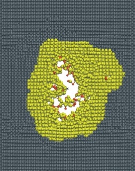
The researchers used a scanning tunneling microscope (STM), a device that images surfaces at an atomic level, in order to determine the success of their doping procedure. These measurements indicated how the Fermi energy of the nanocrystals changed upon doping, a key feature in controlling the electronic properties of electronic devices. The results, notes Prof. Rabani, indicate that the nanocrystals have been doped with both n-type dopants, indicating the presence of excess electrons in the nanocrystals, and p-type, which contribute positively charged holes to the semiconductors. This will allow for their use in electronics that require a pn junction, such as solar panels, light emitting diodes, and more.
Prof. Rabani says that this technology can go a long way. Doping semiconductors, he explains, has been essential for the development of technology. "Parallel to this, we also know we want to make electrical components very small. A big portion of future electronics or optics is going to be based on doping nanoparticles."
For further information: http://www.aftau.org/site/News2?page=NewsArticle&id=14944
Photo: http://web.mit.edu/mbuehler/www/Teaching/LS/si-o2.jpg