
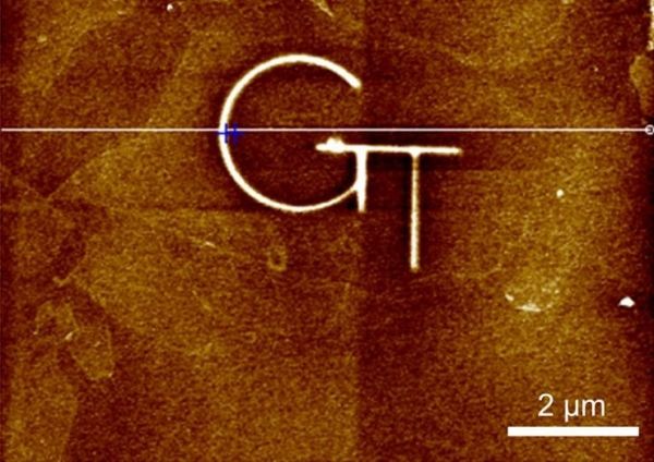
By varying the energy and dose of tightly focused electron beams, researchers have demonstrated the ability to both etch away and deposit high-resolution nanoscale patterns on two-dimensional layers of graphene oxide.
By varying the energy and dose of tightly focused electron beams, researchers have demonstrated the ability to both etch away and deposit high-resolution nanoscale patterns on two-dimensional layers of graphene oxide. The 3D additive/subtractive “sculpting” can be done without changing the chemistry of the electron beam deposition chamber, providing the foundation for building a new generation of nanoscale structures.
Based on focused electron beam-induced processing (FEBID) techniques, the work could allow production of 2D/3D complex nanostructures and functional nanodevices useful in quantum communications, sensing, and other applications. For oxygen-containing materials such as graphene oxide, etching can be done without introducing outside materials, using oxygen from the substrate.
“By timing and tuning the energy of the electron beam, we can activate interaction of the beam with oxygen in the graphene oxide to do etching, or interaction with hydrocarbons on the surface to create carbon deposition,” said Andrei Fedorov, professor and Rae S. and Frank H. Neely Chair in the George W. Woodruff School of Mechanical Engineering at the Georgia Institute of Technology. “With atomic-scale control, we can produce complicated patterns using direct write-remove processes. Quantum systems require precise control on an atomic scale, and this could enable a host of potential applications.”
Continue reading at Georgia Tech.
Image via Georgia Tech.