
True to Moore’s Law, the number of transistors on a microchip has doubled every year since the 1960s. But this trajectory is predicted to soon plateau because silicon — the backbone of modern transistors — loses its electrical properties once devices made from this material dip below a certain size.
True to Moore’s Law, the number of transistors on a microchip has doubled every year since the 1960s. But this trajectory is predicted to soon plateau because silicon — the backbone of modern transistors — loses its electrical properties once devices made from this material dip below a certain size.
Enter 2D materials — delicate, two-dimensional sheets of perfect crystals that are as thin as a single atom. At the scale of nanometers, 2D materials can conduct electrons far more efficiently than silicon. The search for next-generation transistor materials therefore has focused on 2D materials as potential successors to silicon.
But before the electronics industry can transition to 2D materials, scientists have to first find a way to engineer the materials on industry-standard silicon wafers while preserving their perfect crystalline form. And MIT engineers may now have a solution.
The team has developed a method that could enable chip manufacturers to fabricate ever-smaller transistors from 2D materials by growing them on existing wafers of silicon and other materials. The new method is a form of “nonepitaxial, single-crystalline growth,” which the team used for the first time to grow pure, defect-free 2D materials onto industrial silicon wafers.
Read more at Massachusetts Institute of Technology
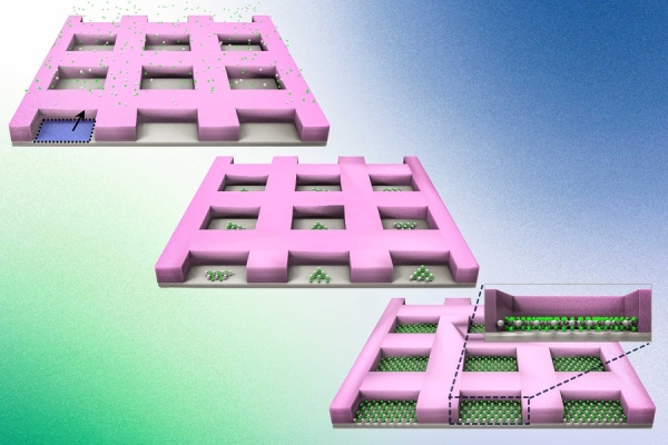
Image: By depositing atoms on a wafer coated in a “mask” (top left), MIT engineers can corral the atoms in the mask’s individual pockets (center middle), and encourage the atoms to grow into perfect, 2D, single-crystalline layers (bottom right). Credits: Courtesy of the researchers. Edited by MIT News.